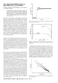
[en] The performance of SiO2/AlGaN/GaN MOSHFETs is described. The C–V measurements showed slight increase in sheet carrier density after applying 12 nm-thick PECVD SiO2. The devices exhibited gate leakage current of 5 .10 ^-10 A/mm. Small-signal RF characterisation of 0.7 mm gate length devices yielded an fT of 24 GHz and an fmax of 40 GHz, which are comparable to those typical for state-of-the-art AlGaN/GaN HFETs.
Disciplines :
Electrical & electronics engineering
Identifiers :
UNILU:UL-ARTICLE-2009-372
Author, co-author :
Bernát, J.; Institute of Thin Films and Interfaces (ISG1) and cni - Center of Nanoelectronic Systems for Information Technology, Research Centre Jülich, 52425 Jülich, Germany
Gregusová, D.; Institute of Electrical Engineering, Slovak Academy of Sciences, SK-84104 Bratislava, Slovak Republic
Heidelberger, G.; Institute of Thin Films and Interfaces (ISG1) and cni - Center of Nanoelectronic Systems for Information Technology, Research Centre Jülich, 52425 Jülich, Germany
Fox, A.; Institute of Thin Films and Interfaces (ISG1) and cni - Center of Nanoelectronic Systems for Information Technology, Research Centre Jülich, 52425 Jülich, Germany
MARSO, Michel ; Institute of Thin Films and Interfaces (ISG1) and cni - Center of Nanoelectronic Systems for Information Technology, Research Centre Jülich, 52425 Jülich, Germany
Lüth, H.; Institute of Thin Films and Interfaces (ISG1) and cni - Center of Nanoelectronic Systems for Information Technology, Research Centre Jülich, 52425 Jülich, Germany
Kordoš, P.; Institute of Electrical Engineering, Slovak Academy of Sciences, SK-84104 Bratislava, Slovak Republic
Language :
English
Title :
SiO2 /AlGaN/GaN MOSHFET with 0.7 µm gate-length and fmax / fT of 40/24 GHz
Publication date :
2005
Journal title :
Electronics Letters
ISSN :
0013-5194
Publisher :
Institution of Electrical Engineers, London, ROYAUME-UNI